Low Temperature Wet Conformal Metal Silicide Deposition for Transistor Technology through an Organometallic Approach
The formation of metal silicides, which are indispensable materials involved in the fabrication of all field effect transistors to reduce the contact resistance of the source and drain regions, has been identified as one of the most critical steps in current fabrication process flows. Among all the existing metal silicides, cobalt silicide (CoSix) has advantages for its low resistivity, its material compatibility, and its good stability1. However, the transition towards devices using advanced 3D geometries makes it challenging to form homogeneous silicides using classical silicidation processes based on sputtering. Therefore, a one-pot wet chemical approach2 has been proposed to synthesize the metal silicide layer onto silicon wafer, exhibiting applicable electric properties and allowing a homogenous coverage of 3D-structure device.
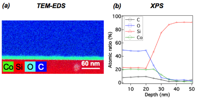
A 20-nm Co-rich layer on Si (100) wafer was observed by electron microscopy (STEM-EDS), a layer that according to preliminary XAS results on the Si(0) model indicated to be CoSix. XPS spectroscopy showed a small amount of carbon contamination, which is similar to what is found for the pristine Si wafer (< 9%, Figure 1). Then, high temperature vacuum-treatment (~10-5 mbar) leads to layer having conductive behavior (Ohmic behavior) with a lower resistivity (ρ=116 μΩ.cm) measured by 4-point probe measurement confirming the presence of Cobalt silicide. In addition to forming the silicide layer onto the flat Si (100) surface, the method was applied to 3D-patterned wafers, in which the TEM results showed that a promising step coverage ratio could be obtained. This work shows that the homogeneous CoSix layer can be deposited via wet organometallic approach at ambient temperature and that, after thermal vacuum-treatment, it exhibits an Ohmic behavior with a low resistivity, thus creating an alternative possibility for modern 3D-transistor fabrication.
[1] Bernal-Ramos, K.; Saly, M. J.; Kanjolia, R. K.; Chabal, Y. J., Atomic Layer Deposition of Cobalt Silicide Thin Films Studied by in Situ Infrared Spectroscopy. Chem. Mater. 2015, 27 (14), 4943-4949.
[2] Lin, T.-H.; Margossian, T.; De Marchi, M.; Thammasack, M.; Zemlyanov, D.; Kumar, S.; Jagielski, J.; Zheng, L.-Q.; Shih, C.-J.; Zenobi, R.; De Micheli, G.; Baudouin, D.; Gaillardon, P.-E.; Copéret, C., Low-Temperature Wet Conformal Nickel Silicide Deposition for Transistor Technology through an Organometallic Approach. ACS Appl. Mater. Interfaces 2017, 9 (5), 4948-4955.